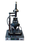
Scanning Probe Microscope Solver EC
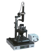
A Solver EC system is intended to perform the electrochemical studies of adsorption layers formation, metals deposition and dissolution in combination with in situ monitoring the electrode/solution interface morphology by STM with atomic scale resolution and tunnel spectros-copy.
The system consists of the following:
- basic SPM controller
- bipotentiostate
- vibration isolation table
- coarse approach (stepping motor having the following parameters…) and sample lateral translation system
- measuring head with a piezoscanner
- electrochemical cell operating under inert atmosphere
The bipotentiostate makes it possible to carry out various electrochemical experiments in potentiostatic, potentiodynamic and galvanostatic modes. Potentials of the working electrode and probe are set independently relative to the reference electrode. The specific universal pro-grammator gives the user practically unlimited opportunities to perform automatized electro-chemical measurements. The electrode polarization program can consist of 10 steps and each of them allows to execute independently various electrochemical actions the required number of times in the given range of current and frequency. For example, during some program steps the electrode preprocessing can be accomplished (potentiostatic polarization with chronoampero-grams registration, linear potential ramp at given rate or cyclic voltamperometry, open circuit stationary potential measurements, etc.) while during other steps it is possible to execute the po-tentiostatic or galvanostatic metals deposition with a series of current transients at different po-tentials registration and automatic recording of measurement results on disc.
The bipotentiostate software provides the user-friendly interface for conducting the electrochemical experiments, data express analysis and processing. One of the instrument features is the ability to use the high quality hemispherical single crystals of noble metals produced in many leading laboratories in the world by Clavilier's method. Di-ameter of such single crystals is normally under 3-4 mm. To use them one needs the electro-chemical microcells of special design which are the components of this instrument.
Bipotentiostat/galvanostat |
Output Compliance Voltage: |
± 15 V |
Voltage Scan Range: |
± 4 V (stability ± 1 mV) |
Current Ranges: |
±5mA; ± 100 uA; ± 2 uA (accuracy of measurement ±0.1 % of the range) |
Reference Input Impedance: |
> 1011 Om |
Modes: |
manual; sweep (1 mV/s to 100 mV/s), pulse (time resolution 10 ms); potentiostatic current transients; cyclic and linear voltammetry; universal programmer. |
Computer: |
Pentium II or higher. |
System: |
Windows 98/XP |
EC Cell |
Material: |
Teflon |
Max size: |
35x10 mm |
Volume of electrolyte: |
0.5 to 1.5 ml |
EC STM Head |
Scanner: |
3x3x1.5 um (12x12x1.5 um), STM tips holder |
Preamplifier: |
± 50 n, noise 3 p. |
Tips |
Material: |
W, Pt-Ir (10-25%) |
Diameter: |
0.4-0.5 mm |
Tip length: |
up to 20 mm |
Isolated part length: |
5-7 mm |
Insulation: |
Insulation: Apiezon Wax. |
Electrodes |
Working: |
disks 4-15 mm (Au (111), Pt (111), HOPG, polished polycrystalline metals) |
Counter: |
Cu-wire, Pt-wire, Au-wire |
Reference: |
Cu-wire, Pt-wire, Au-wire, Ag/AgCl (Cypress system) |
Electrolyte: |
H2SO4 (0.01 M) + CuSO4 (0.01 M) |
System of inert atmosphere ensuring: |
nitrogen, argon |
Acceptance test |
Underpotential deposition of Cu on Au (111); Electrodeposition of Cu on Au (111), Pt (111), HOPG. |
 Printer Friendly Version Printer Friendly Version
Scanning Probe Microscope Solver HV
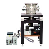
Solver HV is intended for work in high vacuum conditions and controllable gas medium. Measuring head Smena HV is designed by vacuum technology using vacuum compatible materials. The case of the head is without covering. Its wires have no braid and sockets are metallized. To decrease the thermal drift, Smena HV is supplied with a preamplifier with reduced thermal emission and the temperature compensators are installed. Smena HV is supplied with the special motorized approach leg to provide approaching of the probe to the researched sample. It is based of the stepper motor intended for work in conditions of high vacuum. Smena HV head is set to the vacuum chamber on the stage. The stage is supplied with special handles for more comfortable setting and taking out the head with the stage from the vacuum chamber. It is possible to work with measuring head Smena HV in room conditions, as with usual Smena head. For this purpose the scanning unit of Smena HV is connected with SPM Controller directly passing the vacuum chamber using the enclosed extension cord.
Measuring modes
Contact AFM/ LFM/ ResonantMode (semicontact + noncontact AFM)/ Phase Imaging/ Force Modulation (viscoelastisity)/ MFM/ EFM/ Adhesion Force Imaging/Scanning Capacitance microscopy (SCM)/Scanning Kelvin probe microscopy(SKM)/Spreading Resistance Imaging (SRI)/ RM Lithography/AFM
Vacuum value |
10-7 torr |
Pumps |
Combination of Rotary and Turbo molecular pumps |
Pump speed |
340 l/sec (depends on modification of turbopump in use) |
Environment control |
Possibility to treat sample surface by plasma; use of non-aggressive gases (such as O2, H2, etc.) |
Sample size |
~10x10mm |
Scan range |
100x100x4 μm, 50x50x2.5 μm |
Resolution |
Atomic steps resolution |
Optical microscope |
Available for AFM |
Temperature range |
Cooling: helium down to 50K, nitrogen down to 110K
Heating: up to 150°C |
SNOM |
Measuring module realized as a separate flange module |
Magnetic field |
800Oe – 10"; 500Oe -30" |
Printer Friendly Version
Scanning Probe Microscope Solver LS
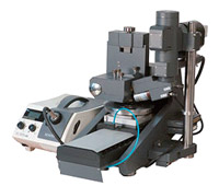
Solver LS is a cutting-edge solution not only for scientific research, but also for production monitoring. With this sophisticated tool you can investigate and control samples (wafers) with the size up to 250mm (300mm optional) in diameter and 15mm thick. The motorized positioning stage and optical viewing system, which are included in Solver LS, allow you to choose any place visually and define a number of areas in different parts of the sample to be scanned automatically. Due to a great number of features Solver LS is abundantly given, the range of application is almost endless.
Product Features
- Thanks to software adjustment of operational modes and functional scheme of the unit, electrical circuit switching can be done without program re-installation.
- The option to save settings in different files allows the user to employ almost all modern methods of scanning probe microscopy.
- An experienced user can develop and implement his or her own techniques including multipass ones.
Sample Size |
Up to 250 mm (300 mm optional) in diameter, up to 15 mm thick |
Scanners |
50x50x2.5 μm (±10%) |
Sample Holders |
Vacuum sample holder for CD/DVD discs, stampers and glass master discs; universal vacuum sample holder for semiconductor wafers (50 - 150 mm) (250 mm optional), CD/DVD stampers, HDD and small samples (min. size is 10mm in diameter) |
SPM Heads |
AFM |
Motorized Positioner |
Linear and rotary translation stages;
linear resolution - 2μm;
bidirectional repeatability - 1μm;
angular resolution - 0.002 degree;
angular repeatability - 0.0014 degree |
Current |
50 pA - 10 nA (linear range), RMS noise 4 pA in 1 kHz bandwidth
10 nA - 10 mA (log range) |
Bias Voltage |
±10 V |
Optical viewing system |
Resolution: 1.5μm
Magnification: with color CCD on 14" monitor 207- 2070
Field of view: max 1.2x0.9 mm, min 120x90 μm
Motorized focus and zoom, control unit
Color CCD camera (SONY SSC-DC50AP 1/2" CCD, 470 TVL), color monitor 14" (SONY SSM- 14N5E horizontal resolution 500 TVL). |
Control system |
SPM Controller |
Vibration Isolation |
Passive isolation is integrated.
Active anti-vibration system is available by request. |
Printer Friendly Version
Scanning Probe Microscope Solver MFM
For many applications it is essential to analyze specimen magnetic properties in a variable external magnetic field by magnetic force microscopy (MFM) in the nanometer scale. For this NT-MDT has launched the new enhancement to its range of atomic force microscopes (AFM) which delivers the complete solution for observation of magnetization reversal processes and other phenomena that depend on magnetic field in the range up to 2 kGauss (0,2 Tesla).
Early experiments include in-situ observations of the domain structure changes of permalloy rectangles, demagnetization process of a hard drive disk, magnetization reversal of a cobalt pattern, variation of anisotropy field across the yttrium iron garnet film thickness etc. You can find more information here.
Product Features
As compared to other models, Solver MFM features all metallic parts of the measuring head and the landing and scanning unit made of non-magnetic materials. This prevents the movement of the probe when switched on or off as well as at the moment the orientation of the magnetic field is modified.
Solver MFM is equipped with the magnetic field generator, creating a magnetic field. The electromagnet is cooled by a water cooling system. The system consists of a liquid thermostat and water cooling hoses.
Sample Size |
Up to 21x3 mm or 21x100x3mm;
Optional: 21x10 mm or 21x100x10mm
Note: The maximum sample size can be either up to 100x20mm, if the electromagnet is not used, or unlimited if the measuring head is used as a stand alone device. |
Scanners |
100x100x5 um (±10%);
50x50x2.5 um (±10%);
150x150x7.5 um (±10%) – operating in the DualScan mode (in the combined scanning-tip and scanningsample). |
Min. Scanning Step |
0.0012 nm; 0.006 nm; 0.0072 nm |
External electromagnet |
Magnetic field |
0,2 T (plus-minus) in the probe-sample interface area during the scanning process. The magnetic field is directed along a sample surface. |
Magnet pole gap |
6mm |
Water cooling |
Water thermostat with temperature control in the range 10 – 300 °C. |
Hall device (magnetic field measurement) |
Optical viewing system |
Resolution 3 μm
Numerical aperture 0.1 μm
Magnification from 58x to 578x
Field of view from 2 to 0.51 mm |
Printer Friendly Version
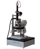
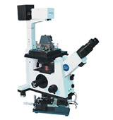
Scanning Probe Microscope Solver Pro
Solver PRO-M is a powerful and well-designed universal scientific SPM applicable to almost all areas that SPM can ever be exploited in. Some features make it unique in terms of electronics capability, probe movement precise measurements, and optical system convenience.
The Solver PRO-M model has been suited to be driven by the new-generation controller. It has been designed to incorporate modern achievements in microelectronics. Elegant module architecture and many new design solutions allowed creating one of the most powerful "brain" that SPM ever possessed. It contains more than 10 000 components from the world-best manufacturers as Analog Devices, Burr Brown etc.
Product Features
Very important feature is that the new controller is perfectly suited to work with high frequencies (up to 5 MHz). Thus it is compatible with high frequency cantilevers that can be required to obtain the best quality images. High frequency compliance measurements are also important to perform AFAM (Atomic Force Acoustic Microscopy) – NT-MDT unique microscopy technique for imaging samples with differences in local stiffness. The controller is also designed to process capacitive sensors feed-back signal providing precision scanning.
Parameters |
Type of scanning |
Scanning by sample |
Scanning by probe |
Sample size |
Up to 40x4010 mm
Up to 12x12x2 mm with the liquid cell use |
Up to 100x10020 mm and unlimited for measuring head used for stand alone operation |
Scanners |
3x3x2.6 um (±10%);
10x10x4 um (±10%),
50x50x5 um (±10%) |
50x50x5 um (±10%);
100x100x7 um (±10%);
100x100x10 um (±10%) (only for Shear Force) |
Min. scanning step(DAC) |
0.0004 nm;
0.0011 nm;
0.006 nm |
0.006 nm;
0.012 nm;
0.012 nm |
SPM heads |
AFM
STM: 30 pA-50
nA, RMS noise 4 pA (standard preamplifier); 10 pA-5 nA, PMS noise
1.5 pA (low current preamplifier) |
AFM
Shear Force |
Optical viewing system |
Resolution |
1 um |
Numerical aperture |
0.28 |
CCD |
230 x 2900 x |
Horizontal field of view |
1.2, 0.1 mm |
XY sample positioning |
55 mm |
Positioning resolution |
readable resolution-5 um
sensitivity-2 um |
Heating |
130 ! |
Vibration isolation |
Active vibration isolation system:
Active damping (0.6-100 Hz), >100 Hz - passive damping
Electric shielding and acoustic isolation is provided by the special cast metall hood |
Printer Friendly Version
Scanning Probe Microscope Solver SNOM
Scanning Near-Field Optical Microscopy (SNOM) is one of a number of types of Scanning Probe Microscopy (SPM). This is very powerful modern technique for surface investigation, which can provide the resolution about 50 nm. This resolution is much better than the max. standard optical resolution (500 nm) due to so-called near-field effect. The main idea of SNOM is to measure the light intensity within the distance about 10 nm (much smaller than the wavelength of light) from the sample with the very diminutive probe (sharpened optical fiber tip). This method allows to obtain data of optical properties of the sample surface, to make nanolithograthy, to measure local spectrum on the surface (e.g. quantum dots spectrum), to control the quality of optical surfaces (e.g. mirrors, lens, prisms, splitters etc.), to measure local fluorescence, to obtain the distribution map of light intensity on semiconductor samples. Solver SNOM system is based on inverted optical microscope and with additional measuring heads is easily transformed to Solver BIO model that is widely used for biological applications.
Product Features
- Multi-purpose instrument: SNOM, Shear Force, AFM, STM;
- SNOM Modes: Reflection, Transmission (to be supplied with inverted optical microscope Olympus IX-70 (IX-50) or Biolam-P);
- Scan range: 80x80x4m; - Feedback control: non optical Shear Force scheme;
- Resolution: <100nm; - Inverted Optical Microscope: Olympus IX-70, 50 or Biolam-P; Complete modular design.
SNOM Operation |
Reflection (probe induces the light on the surface, special objective Reflection Mode with the use of inverted microscope optical scheme), Transmission, Shear Force |
Photodetectors |
PMT (Hamamatsu) |
Lasers |
532 nm, 10 mW;
Multi line: 514nm/55mW, 488nm/55mW, 476nm/7mW, 465nm/7mW, 457nm/5mW , 150mW;
Semiconductor Extra input for external laser |
Scan type |
By Probe |
X,Y sample positioning |
30x30mm (within 30mm circle) |
Fine tip positioning |
4x4mm with 5um resolution |
Sample Substrate |
Coverslips, standard slides and other flat samples up to 75x25mm
Petri dishes 35-45mm and 55-60mm |
Inverted Optical Microscope |
Own optical scheme for Olympus IX-70(50), Biolam-P (optional) |
Probes |
Red and Green, aperture < 100nm |
Control System |
SPM Controller |
Vibration Isolation |
Passive isolation is integrated
Active anti-vibration system is available by request |
Printer Friendly Version |