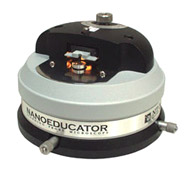
Scanning Probe Microscope Nano Educator
Scientific training laboratory of nanotechnology for institutes and universities
Complex approach to educational process
- Students oriented
- User friendly interface
- SPM techniques step-by-step mastering
- Clearness, animated support
- No complicated adjustments
- Inexpensive consumed materials
- Simple probe replacement
- Probe recovery availability
Basic operation modes
- AFM
- Semicontact modes
- Topography imaging (constant force mode)
- Phase imaging
- Force imaging (constant height mode)
- Force spectroscopy
- Operation in liquids
- AFM lithography
- Dynamic plowing lithography (force)
- STM
- Topography imaging (constant current mode)
- Differential contrast (modulation in X-Y plane)
- Current imaging (constant height mode)
- Work function measurements (Z modulation)
- Tunnel spectroscopy (dI/dV measurements)
- Operation in dielectric liquids
Parameter |
Sample size |
diameter up to 12 mm |
Sample thickness |
up to 3 mm |
Scan range |
70x70x10 m (+/-10%) |
Scanner nonlinearity |
2% |
Min. scanning step |
1 Å |
Max. scan points |
1024x1024 (max. RAM 64 MB) |
Resolution |
AFM mode |
X_Y – 10 nm, Z – 3 nm |
STM mode |
X_Y – 10 nm, Z – 2 nm |
Probe characteristics |
Material |
Tungsten wire D 100 – 150 m |
Tip curvature radius |
100 nm |
Tip cone angle |
20 – 40° |
Tip sharpening availability |
up to 10 nm |
Optical system |
CCD camera for visual tip approach control |
Scanning |
by sample |
Probe is grounded |
Compatibility with long focus optical microscope |
|